FPC / R-Flex Design
Rigid-Flex circuit board is the advanced technology
for next generation of electronics.
Design Capability
As printed circuit board technologies improve and electronics continue to get smaller and smaller, you need to make sure your current circuit board supplier has the appropriate equipment needed for the specialty processes that are found in more advanced circuit board designs. If your application requires a complex multi-layer board with fine lines and traces having plug via requirements, then we got you covered.
Our advanced multilayer Rigid-Flex circuit technology allows for designers to sequentially add additional pairs of layers to form a multilayer PCB up to 20 layers. JinSung Electronics has been very specialized and is a leading company over Rigid-Flex circuit globally, and we have supplied up to 20 layers R-Flex circuit boards to more than 50 customers since 2015.
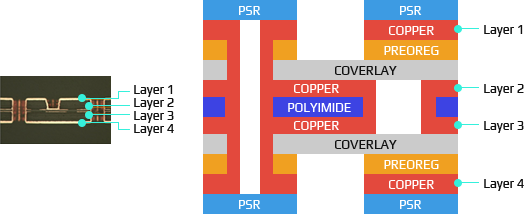
The Rigid-Flex circuit board is a board consisting of a rigid part (non-bending part) and a flex part (bending part), and 3D circuit connection is possible by flexing the flex part. In addition, it has a bendability of up to 150,000 consecutive bends, and it is advantageous for miniaturization and weight reduction because there is no need for a connector for connection between modules.
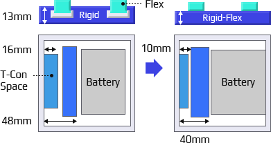
In addition, it is possible to maximize the space utilization in the set with high design freedom,
and a structural design with high density, thinness, and various floors is also possible.
Major application fields : Smartphones, tablets, laptops, wearables, display modules, camera modules, etc.
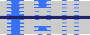
Major advantage of Rigid-Flex circuit board
|

|
|
|
|
|
What core technology JinSung has for developing Rigid-Flex circuit board?
|
We produce HDI/BGA/FCB products, and we can develop advanced technologies and create synergy through technology convergence and integration of each product.
|
|
|

|
What core technology JinSung has for developing HDI circuit board?
-
What is the HDI PCB?
HDI PCB is the Abbreviation of high-density interconnect printed circuit board, a kind of printed circuit board manufacturing technology. An HDI PCB is a circuit board with a relatively high circuit density that uses micro-blind and buried “via”—or the copper-plated holes in PCBs—technology. HDIs are compact products designed for small-capacity users, as they cost much more than standard PCBs.
HDI PCB boards, one of the fastest growing technologies in the PCB industry, are now available at JinSung Electronics. HDI PCBs contain both the blind via and buried via hole varieties and have a higher circuitry density than traditional circuit boards.
-
What is the JinSung’s capability to develop HDI PCB?
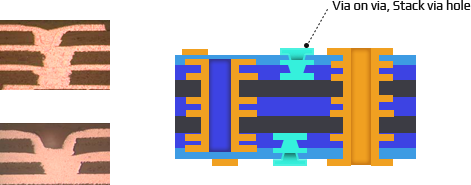
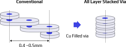
A microvia maintains a laser-drilled diameter of, typically, 0.006" (150µm), 0.005″ (125µm), or 0.004" (100µm), which are optically aligned and require a pad diameter of typically 0.012" (300µm), 0.010" (250µm), or 0.008" (200µm), allowing additional routing density. Microvias can be via-in-pad, offset, staggered or stacked, non-conductive filled and copper-plated over the top, or solid copper filled or plated. Microvias add value when routing out of fine-pitch ball grid arrays (BGAs) such as 0.8 mm pitch devices and below.
Additionally, microvias add value when routing out of a 0.5 mm pitch device where staggered microvias can be used. However, routing micro-BGAs such as a 0.4 mm, 0.3 mm, or 0.25 mm pitch device, requires the use of Stacked MicroVias using an inverted pyramid routing technique.
-
What are HDI PCB Advantages?
- HDI technology can reduce the cost of PCB, although when the density of PCB increases beyond eight layers, it will be more expensive to manufacture with HDI.
- Have better electrical performance and signal accuracy
- Better reliability
- Can improve thermal properties
- Can improve radio frequency interference/electromagnetic wave interference/electrostatic discharge (RFI/EMI/ESD)
- Greater design efficiency
FPC/R-FPC Design capability
-
Single Side
Item Spec Pattern Width Min. 45㎛ Space Min. 45㎛ Thickness 0.05T Stiffner PI, SUS, EPOXY.. Other EMI, D/T.. 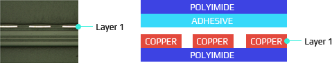
-
Double Side
Item Spec Drill Min. 0.08㎛ Pattern Width Min. 50㎛ Space Min. 50㎛ Thickness 0.11T Stiffner PI, SUS, EPOXY.. Other EMI, D/T.. 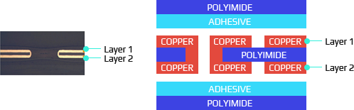
-
Multi-Layer (HDI) / Rigid-FLEXIBLE
Item Spec INNER Pattern Width Min. 45㎛ INNER Pattern Space Min. 45㎛ Machince Drill Min. 0.15mm Laser Drill BVH Min. 0.1mm Cu Plating 25[+-3㎛] / Via Fill / CAP PLATING OUT Pattern Width Min. 60㎛ OUT Pattern Space ~20 LAYER LAYER 0.25T~3.0T Thickness 0.25T~3.0T Stiffner PI, SUS, EPOXY .. Other EMI, D/T ..